Perovskite Based Charge Transport Layers for Thin Film Optoelectronic Devices
- Pending
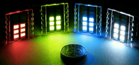
Light-emitting diodes (LEDs) and organic light-emitting diodes (OLEDs) are used widely in solid state lighting, electronic displays, bio-imaging, and photovoltaic (PV) applications. A cheaper, more efficient LED device can impact multiple markets. Some of the primary applications include television displays, mobile device displays, medical applications, solid state lighting, and energy applications.
This LED technology comprises two components—an LED device and the process of manufacturing that device. The LED device comprises earth-abundant materials. The manufacturing process takes place at room temperature using simple starting materials and common organic solvents in a single container. The color of the LEDs can be tuned.
Typically, thin film optoelectronic devices, such as LEDs and PVs, are configured with a layered structure. This includes a photoactive (either light emitting or light harvesting) layer sandwiched between charge transport layers that contact with electrodes. These charge transport layers play a crucial role in efficiency of the entire device.
This technology uses perovskite materials to create cost effective, efficient charge transport layers.